
“Hands off” approach to looking into silicon chips
London, UK
The possibility of looking inside silicon chips to see their remarkably small working parts, without damaging the chips, is a step closer thanks to an international consortium led by BNC.
Working as part of the Nanomicrowave consortium (www.nanomicrowave.eu) funded through the European Union’s Framework-7 program, the international team has demonstrated the ability to generate pictures of tiny three-dimensional components, made from phosphorus atoms, that are completely invisible to all other imaging technologies.
Remarkably, the pictures of these components were obtained even though the components were only the size of a few tens of atoms, were atomically thin and were buried under the surface of the chip. An accurate quantitative determination of the location of the buried components was obtained, along with certain electrical properties. This breakthrough has been published in the 28 June 2017 edition of Science Advances (goo.gl/vr6eU5).
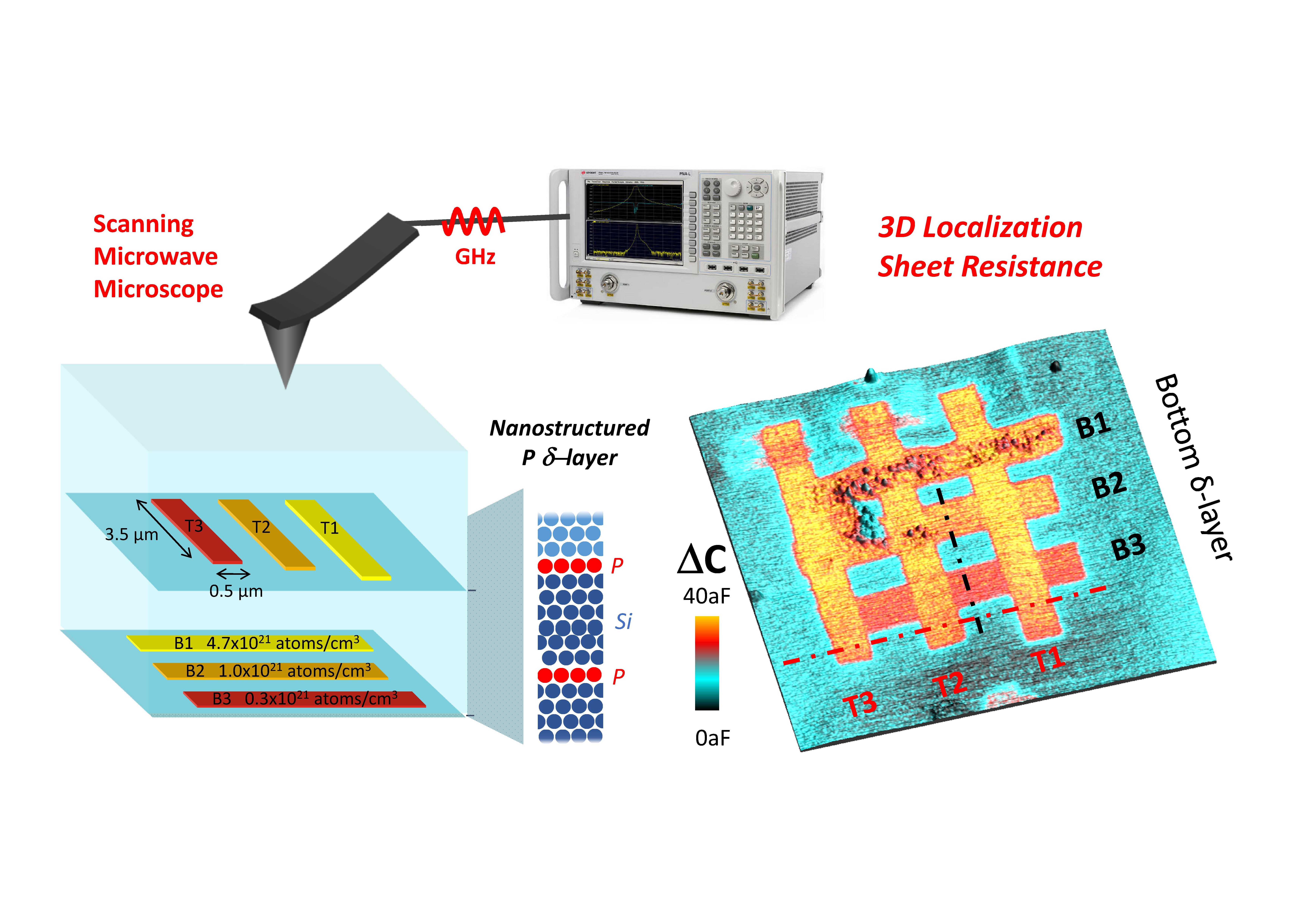
One of BNC’s long-term research partners, the London Centre for Nanotechnology (LCN) at University College London (UCL), contributed significantly to the study. The components that were studied, including a three-dimensional criss-cross of metallic phosphorus stripes, were designed and manufactured by UCL PhD student Alex Klker. He used a super-sharp metal needle to write patterns in a single layer of hydrogen atoms that lay on the surface of a silicon chip, creating a template of a desired shape. By causing a chemical reaction to happen between the surface of the chip and phosphine gas, phosphorus atoms were written into the surface, in the shape of the template. The phosphorus structures were then buried with more silicon to complete the device.
A recently developed scanning microwave microscope was used to take pictures of the components, obtained with our collaborators at Johannes Kepler University (JKU), led by Georg Gramse, and by Keysight Technologies (Austria), Paul Scherrer Institut, ETH Zürich and EPF Lausanne (Switzerland). The microscope works by focussing microwaves (like those from a microwave oven), to the end of a metal tip which is pushed against the surface of the chip. The microwaves are fired into the chip, subsequently bouncing back from the buried components, measured, and used to construct a picture.
http://www.scienceandtechnologyresearchnews.com/hands-off-approach-looking-silicon-chips/
According to the LCN’s Dr Neil Curson “The work is potentially of global significance because silicon chips are becoming so sophisticated and intricate that taking snapshots of their smallest working parts is incredibly difficult and time consuming, and currently involves destroying the chip. If we could easily see all components of a chip, in a non-destructive manor, it would be a game-changer. What we have done is a big step towards just that. Such technologies are also becoming important for governments who are interested in knowing what is inside the foreign electronics they are using!”
“Another important application of our imaging technology is in assisting in the fabrication of phosphorus-in-silicon quantum computers, which have the potential to revolutionise computing completely, if realised.”
Dr Ferry Kienberger from Keysight Technologies says, “Our company sees this work as a major breakthrough in demonstrating that scanning microwave microscopy is the way forward for the characterisation of the next generation of electrical devices and quantum components in silicon.”
Commenting on the breakthrough, BNC’s CEO Dr David Sarphie said, “We are thrilled to have contributed in a major way to this work and are thankful for the support we received from the EU’s Framework-7 Initial Training Network (ITN) programme that made this international consortium of experts possible. The ability to work with world-leading universities, companies and institutes from around Europe is key to the success of research collaborations like Nanomicrowave.”
About Bio Nano Consulting
Bio Nano Consulting specialises in delivering innovative solutions to industry across the life sciences and technology sectors. In addition, as an SME it plays a key role as coordinator in European Framework-7 and Horizon 2020 programmes. BNC was the first consultancy in Europe to focus on the interface between bio and nanotechnology, and it continues to provide product development, project management and strategic consultancy to a broad range of international clients.
About UCL
UCL is a world-class university; with academic strength in breadth and depth. UCL offers an enormous range of taught programmes at undergraduate and postgraduate level, alongside exceptional postgraduate research opportunities. UCL’s global eminence is recognised through its top seven world ranking (QS World University Rankings 2016/17). In the last Research Excellence Framework (December 2014), UCL was the top-rated university in the UK for research strength, by a measure of overall quality of research multiplied by the number of staff submissions.
About Keysight
Keysight, is a US company that manufactures test and measurement equipment and software. In 2014, Keysight was spun off from Agilent Technologies, bringing with it the product lines focused on electronics and radio, leaving Agilent with the chemical and bio-analytical products.
Find us on:


